
AIdataNewsGlobal General: CXMT Targets HBM3E Mass Production by End-2026 as China Pushes on AI Memory Supply
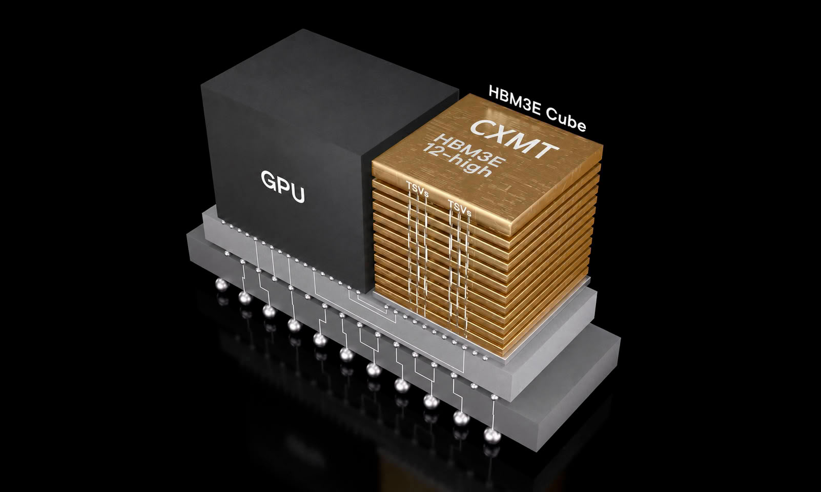
A domestic Chinese memory supplier is moving from prototype-like testing toward a production decision for advanced AI memory. ChangXin Memory Technologies, known as CXMT, is said to be preparing HBM3E for mass production within the next two months, while pointing to a formal start window by the end of 2026. The company already completed a risk trial in August of this year and delivered customer samples, according to industry information. This briefing summarizes the cited production plan, the technical parameters that define HBM3E, the remaining yield constraints and the questions readers may watch next.
Key facts from the CXMT HBM3E update
- CXMT is expected to move HBM3E toward mass production within the next two months, with a formal start target by the end of 2026.
- The project already passed a risk-trial step in August of this year, and customer samples have been delivered for testing.
- HBM3E is described against JEDEC standards, using a 1024-bit bus architecture and capacity configurations spanning 24GB to 36GB.
- Yield is the central obstacle, with reported overall yield around 20% to 30%, while leading international suppliers are viewed as having a clearer advantage.
- For domestic AI hardware, the value of a Chinese HBM source is tied to supply pressure, customer validation and future accelerator product plans.
Where CXMT says the production path stands
The reported plan places CXMT in a bridge phase: risk production has started, samples are in customer hands, and the company is preparing a commercial ramp. The timing is cautious, because the target is not simply to demonstrate an HBM3E package but to enter production with stable quality. The near-term product emphasis is on 8-stack HBM3E, also described as 8-layer stacking. The same source environment suggests the company is not expected to push rapidly toward the larger-capacity 12-stack, or 12-layer stacking, version, even though those forms are common in the broader HBM market.
Reported HBM3E parameters
| Reported HBM3E parameter | Cited value | Context from the update |
|---|---|---|
| Standards reference | JEDEC | The technical envelope for HBM3E is tied to the standard. |
| Bus architecture | 1024-bit | The wide bus supports the high bandwidth required by AI accelerators and data-center GPUs. |
| Per-pin transmission rate | 9.2Gbps to 12.4Gbps; 9.6Gbps is common | These rates shape performance expectations for the memory subsystem. |
| Aggregate bandwidth | about 1.2TB/s | The bandwidth level is relevant to training and running large AI models. |
| Capacity options | 24GB to 36GB | The cited range shows the configurations discussed for HBM3E. |
| Stacking formats | 8-stack and 12-stack | Both are described as mainstream, with 8-layer stacking and 12-layer stacking as the corresponding forms. |
How to read the parameter table
The table translates the cited HBM3E profile into a concise checklist. Each line is limited to what the update states; the purpose is to help General readers distinguish design targets from production constraints. The distinction matters because a memory product can satisfy a standard-defined architecture while still facing yield, packaging or customer-validation hurdles before mass production.
Yield, TSV stacking and the manufacturing bottleneck
Mass production is not guaranteed by a product definition alone. The reported constraint is yield, especially the difficulty of vertically stacking multiple DRAM dies with TSV technology. TSV, or through-silicon via, creates vertical connections, but the process raises manufacturing and packaging complexity. According to the cited industry view, HBM3E still faces yield issues, and that directly affects capacity expansion. The reported overall yield is about 20% to 30%. The front-end wafer manufacturing stage is said to reach about 30%, while the back-end packaging stage can increase the pass rate by about 70%. Final overall yield still needs to improve before the company can move from sample validation to stable supply.
Stacking maturity is one of the most important comparisons. The update notes the following differences:
- Samsung used about 5000 TSV connections in a single layer during the HBM2 era.
- SK hynix exceeded 8000 TSV connections in HBM3 products.
- CXMT is trying to realize an HBM3E design with about 3000 TSV connections, which places higher demands on manufacturing precision and reliability.
Customer samples and performance positioning
Multiple message sources reported that CXMT has sent two versions of HBM3E samples to domestic AI chip companies. One version is described as standard, while the other is a newer version optimized for yield. These samples are now in customer-side testing and validation. Early test information suggests that the current product's overall behavior is closer to SK hynix's previous-generation HBM3 than to the most advanced international HBM3E offerings. Industry commentary argues that for a manufacturer newly entering the HBM track, reaching mass production itself would already be a major breakthrough, even if the product is not yet at the leading edge.
Why China's AI memory supply chain cares
HBM is one of the most critical storage technologies inside AI accelerators, data-center GPUs and high-performance computing systems. Compared with traditional DRAM, it provides much higher bandwidth, making it indispensable for training and running large AI models. The global market is currently dominated by SK hynix, Samsung Electronics and Micron, so any new production source is examined for both technology level and supply reliability.
- SK hynix, Samsung Electronics and Micron are cited as the dominant global HBM suppliers.
- CXMT is the domestic Chinese memory maker being watched as a potential new HBM source.
- Alibaba T-Head and Cambricon are cited as domestic AI chip companies that have previously tested domestic HBM solutions.
Analysts say CXMT can still have motivation to advance mass production despite current yield challenges. The reason is demand-side: Chinese AI chip companies are seeking larger supplies of high-bandwidth memory, and a local HBM source is becoming more important. Tight advanced AI memory supply and import-restriction pressure have helped create clear domestic demand for HBM products. Recent market observations have pointed to AI chip price increases, and HBM supply is widely considered one important reason. Alibaba T-Head and Cambricon have previously been reported to test domestic HBM solutions, a step described as aimed at reducing reliance on overseas supply chains.
What comes next: validation, ramp-up and ecosystem impact
The next checkpoints are narrow and concrete: whether the production preparation within the next two months becomes a real start, whether August-of-this-year trial learning converts into stable yields, and whether customer validation opens the path to accelerator products. If customer checks proceed smoothly, domestic AI accelerator products using CXMT HBM3E could enter the market as early as 2027. The comparison remains uncomfortable: the gap is described as one to two generations versus global leading suppliers. Yet the strategic effect is still visible in the update: CXMT's entry into HBM means China's local AI hardware ecosystem is working to complete a key missing component and to challenge the high-end AI memory market.
FAQ
What is CXMT trying to do?
CXMT is preparing to bring HBM3E into mass production within the next two months, with a reported formal start window by the end of 2026. The company already performed a risk trial in August of this year and delivered customer samples.
Why does HBM3E matter for AI infrastructure?
HBM supports AI accelerators, data-center GPUs and high-performance computing systems. It provides much higher bandwidth than traditional DRAM, which is needed for training and running large AI models.
What are the main technical limits?
The main limits are yield and TSV stacking maturity. Reported overall yield is about 20% to 30%, while the front-end wafer stage is around 30% and back-end packaging can raise the pass rate by about 70%. TSV connection counts, manufacturing precision and reliability remain central challenges.
How close is the product to the global market?
Early testing suggests performance is closer to SK hynix HBM3 than to the most advanced international HBM3E products. The gap is described as one to two generations versus leading suppliers, while mass production itself would still be a major breakthrough for a new entrant.
CXMT's HBM3E effort is therefore best read as a supply-chain milestone rather than a finished product race. The decisive question is whether risk-production learning, customer validation and TSV yield improvement can converge fast enough to support domestic AI accelerator adoption around 2027.