
Nvidia’s 8-Layer HBM4 Reassessment for the Rubin Series: Samsung and SK hynix Balance Cooling, Yield and Supply
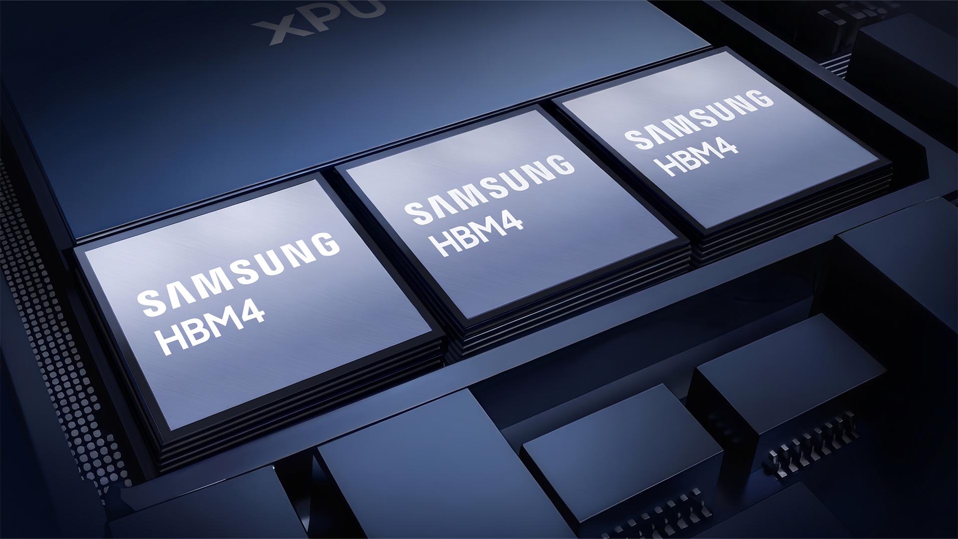
Manufacturability, rather than peak specification, appears to be the central question behind recent supply-chain discussions involving Nvidia, Samsung and SK hynix. In the third quarter of 2026, those conversations reportedly turned toward using a larger share of 8-layer HBM4 configurations in future products. The shift does not erase interest in 12-layer HBM4 or HBM4E, but it shows how cooling, bonding defects and wafer yield can reshape assumptions about the Rubin series.
Checklist: what the reported Nvidia memory discussion covers
- Nvidia reportedly began discussions with Samsung and SK hynix in Q3 2026 about future products adopting more 8-layer HBM4 configurations.
- Market expectations had leaned toward 12-layer HBM4 or HBM4E as the dominant memory path for the Rubin series.
- The reported reconsideration is tied to production realities, especially thermal resistance, wafer-bonding defect risk and yield.
- 8-layer stacking offers lower capacity per stack than taller alternatives but is presented as an easier manufacturing and cooling compromise.
- 12-layer HBM4 products are not being dropped: Samsung and SK hynix are still reported to be in mass production and have Nvidia certification.
- Over the next few years, 12-layer HBM4 is expected to remain important, while the 8-layer version may gain significant share from mid-2027.
- South Korean media disclosures indicate Samsung and SK hynix must obtain independent certification for 8-layer HBM4.
- Nvidia is also reported to be evaluating 8-layer HBM4E; the final choice will reflect Rubin Ultra and NVL rack-scale system design requirements, supply capability and total cost structure.
The reported configuration review can be read as a signal that high-end AI hardware decisions are increasingly shaped by repeatable factory outcomes, not only by the number of memory layers on paper.
Data snapshot: how layer count changes the reported trade-off
| Reported item | 12-layer HBM4 path | 8-layer HBM4 path |
|---|---|---|
| Manufacturing pressure | Taller stacking is associated with more difficult production; for every one layer added, thermal resistance rises, cooling becomes harder and wafer-bonding defect probability increases. | Lower stacking complexity is described as the main advantage; the reported view is that it is easier to produce and cool. |
| Yield expectation | The reported concern is that overall yield can fall as more layers are added. | The 8-layer scheme is positioned as a compromise that supports yield and stability, although the per-stack capacity trade-off remains. |
| Commercial status | Samsung and SK hynix are reported to be mass-producing 12-layer HBM4 products and have secured Nvidia certification. | Samsung and SK hynix are reported to be preparing components, materials and quality validation to obtain independent certification for 8-layer HBM4. |
| Market role | Expected to remain an important part of the high-end HBM market over the next few years. | Market share of the 8-layer version is expected to rise significantly starting from mid-2027. |
Why thermal behavior and bonding defects sit at the center
The reported technical premise is straightforward: layer count is not a neutral specification. In DRAM stacks, each added layer increases the amount of heat that must move through the package and adds more interfaces where bonding-related defects can appear. For Nvidia, Samsung and SK hynix, the issue therefore becomes whether the product roadmap can be supported by reliable volume production, not merely by advanced architecture diagrams. That makes 8-layer stacking attractive as a balanced option: it accepts a capacity compromise in exchange for simpler fabrication and thermal management.
Capacity compromise does not mean the option disappears
For the Rubin series, the reported move toward more 8-layer HBM4 use does not suggest that 12-layer HBM4 is becoming irrelevant. The reporting maintains that current 12-layer HBM4 products remain in mass production and have already received Nvidia certification. The reported facts point to a configuration mix rather than a full replacement: 12-layer products continue serving high-end demand, while the 8-layer version becomes more visible if manufacturers can secure certification and if Nvidia’s design choices favor cost and supply stability.
Independent certification is a separate step for 8-layer HBM4
South Korean media disclosures also introduce a separate qualification milestone: Samsung and SK hynix still need to obtain independent certification for 8-layer HBM4. The companies are reported to be preparing parts, materials and quality validation processes. Because the 8-layer scheme is less technically complex than the 12-layer scheme, industry participants cited in the reporting see certification as less difficult and unlikely to cause a major delay.
Rubin Ultra and NVL rack-scale systems keep the configuration debate open
The final memory choice is still described as an assessment rather than a decision. Nvidia is reported to be evaluating not only 8-layer HBM4 but also 8-layer HBM4E. The outcome will be tied to Rubin Ultra, as well as the NVL rack-scale system, and will depend on design needs, supply availability and the overall cost structure. In other words, the configuration may vary according to the requirements of different Rubin-era system targets.
Platform context: Rubin and Rubin Ultra follow Blackwell series
The reported HBM4 configuration review is part of a broader product cycle. Rubin and Rubin Ultra are planned for 2027 as the next-generation AI computing platforms intended to succeed the Blackwell series as Nvidia’s flagship direction. The memory layer choice therefore sits inside a larger design question about how to deliver that transition without adding unnecessary manufacturing risk.
FAQ: the most likely reader questions about the reported HBM4 change
Is 12-layer HBM4 being abandoned?
No. According to the reports, Samsung and SK hynix are still producing 12-layer HBM4 products, and those products have obtained Nvidia certification. 12-layer HBM4 is expected to remain an important part of the high-end HBM market over the next few years.
Why would Nvidia look at 8-layer HBM4?
Because manufacturing difficulty can outweigh specification height. The reported reasoning is that adding one layer at a time increases thermal resistance, complicates cooling and raises the chance of wafer-bonding defects, which lowers overall yield. The 8-layer stack is presented as a trade-off that improves manufacturability, cost balance and supply stability.
Is 8-layer HBM4E also under consideration?
Yes. The reports say Nvidia is evaluating 8-layer HBM4E in addition to 8-layer HBM4. The eventual configuration will depend on Rubin Ultra and NVL rack-scale system design requirements, supply capacity and total cost structure.
Has Rubin Ultra’s design changed as well?
Yes. The reported adjustment moves Rubin Ultra away from more aggressive, larger-scale chiplet plans and toward a dual-chip design. The stated objective is to reduce manufacturing risk and keep mass-production timing intact.
When could the shift become visible?
From mid-2027, the 8-layer version is expected to gain a significantly larger share, even while 12-layer HBM4 products continue to serve high-end market needs over the next few years.
Outlook: supply reality enters the Rubin roadmap
The reported 8-layer HBM4 review frames Nvidia’s Rubin series as a roadmap decision in which memory architecture, packaging yield and factory throughput are inseparable. For Samsung and SK hynix, independent certification and volume quality remain the immediate hurdles. For Nvidia, Rubin Ultra and its NVL rack-scale system provide the design context that will decide how much 8-layer HBM4, or possibly 8-layer HBM4E, is used. Across the wider industry, the move suggests that next-generation AI platforms will be shaped by the balance between performance ambition and the practical limits of manufacturing.