
AIdataNewsGlobal General: TetraMem MLX300 Tapeout Moves Multi-Level RRAM A-IMC Into a 12 nm FinFET Generation
A tapeout milestone is the kind of event that AI infrastructure watchers tend to read as a progress marker rather than a product announcement. In this update, the company named is TetraMem, and the chip named is MLX300. The reported architecture is analog in-memory computing, or A-IMC, built on multi-level RRAM, with the node designation written as 12 nm in the headline and as 12-nm in the technical description.
The development environment is also part of the reported milestone. The work used Synopsys EDA software, delivered through Synopsys Cloud FlexEDA, and the summary presents that combination as the step that carries multi-level RRAM AI-chip work into a more advanced FinFET node.
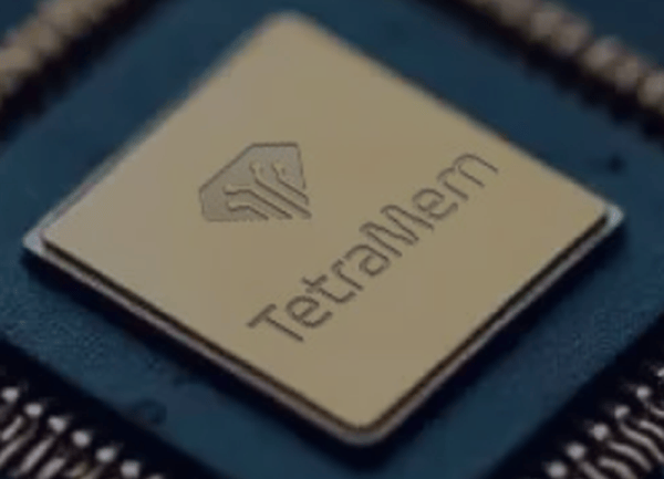
What is being reported, and what is not
- Milestone: MLX300 has completed tapeout.
- Architecture: analog in-memory computing based on multi-level RRAM.
- Node: 12 nm designation in the headline; 12-nm implementation in the technical summary.
- Design tool path: Synopsys software supplied through Synopsys Cloud FlexEDA.
- Lineage: it follows the MLX200/MLX200M full-mask tapeout in 2026 on a commercial 22-nm process.
- Reported chip role: a single-chip accelerator aimed at audio, vision, and smaller language models.
- Reported capacity: up to 64 million INT4 parameters on-chip without external DRAM for model-weight storage.
- Reported efficiency target: energy efficiency exceeding 50 TOPS/W.
How the story connects to the earlier chips
The MLX300 milestone does not appear in isolation. The background anchor is TetraMem’s earlier MLX200/MLX200M family of multi-level RRAM A-IMC SoCs. That earlier step is described as a full-mask tapeout completed in 2026, using a commercial 22-nm process. The newer MLX300 summary then shifts attention to the smaller node and to the use of Synopsys EDA through Synopsys Cloud FlexEDA.
The design logic at a glance
| Element | Reported function or claim |
|---|---|
| Multi-level RRAM | The memory technology underlying the analog in-memory computing SoC described in the update. |
| Scalable architecture | The company intends the architecture to make scalable AI accelerator development easier. |
| Performance per watt | The stated architectural aim includes improving performance per watt. |
| Data movement | The stated architectural aim also includes reducing data movement. |
| Single-chip accelerator | The packaging described for MLX300 targets audio, vision, and smaller language models. |
| On-chip parameter capacity | The figure stated is up to 64 million INT4 parameters on-chip without external DRAM for model-weight storage. |
| Energy-efficiency target | The target quoted in the report is exceeding 50 TOPS/W. |
Why the node transition matters for readers
For a general AI industry audience, the most straightforward takeaway is the sequence: a prior multi-level RRAM A-IMC design at 22-nm, followed by a newer design described as 12-nm. That progression connects two concrete pieces of the story, MLX200/MLX200M and MLX300, while also tying the development to Synopsys Cloud FlexEDA as the named software delivery path.
The second takeaway is the stated system consequence. The article does not simply describe a smaller node; it describes an architecture intended to improve performance per watt, reduce data movement, and keep model weights resident on-chip up to the reported 64 million INT4 parameters. The energy target exceeding 50 TOPS/W is therefore presented as part of the same package, not as an isolated number.
FAQ: What should readers ask next?
Is this a product launch?
No. The reported milestone is tapeout completion for MLX300. The update does not present the chip as shipping, available, or installed in customer systems.
What does the 12-nm detail add?
It marks the newer process node mentioned in the MLX300 summary, especially when compared with the earlier 22-nm full-mask tapeout work involving MLX200/MLX200M in 2026.
Why is Synopsys Cloud FlexEDA named?
It is the delivery route identified for the Synopsys EDA software used in the design work. The mention connects the development tool environment to the milestone itself.
What does “without external DRAM” mean in this report?
In this summary, the absence of external DRAM is tied specifically to model-weight storage: the report says up to 64 million INT4 parameters can be held on-chip without external DRAM for that purpose.
What does the 50 TOPS/W figure represent?
It is described as a target energy efficiency exceeding 50 TOPS/W for the design, not as an independently measured shipping-product result.
Closing read
The AIdataNewsGlobal General view is that this update is best understood as a three-part signal: a chip name, MLX300; a process move, from a 2026 22-nm full-mask tapeout baseline associated with MLX200/MLX200M to a 12 nm headline designation and 12-nm implementation description; and a tooling detail, Synopsys EDA provided through Synopsys Cloud FlexEDA. The reported performance logic remains tied to multi-level RRAM, scalable accelerator development, reduced data movement, on-chip parameter capacity, and the stated efficiency target exceeding 50 TOPS/W.